Originally published: Sep 16, 2019
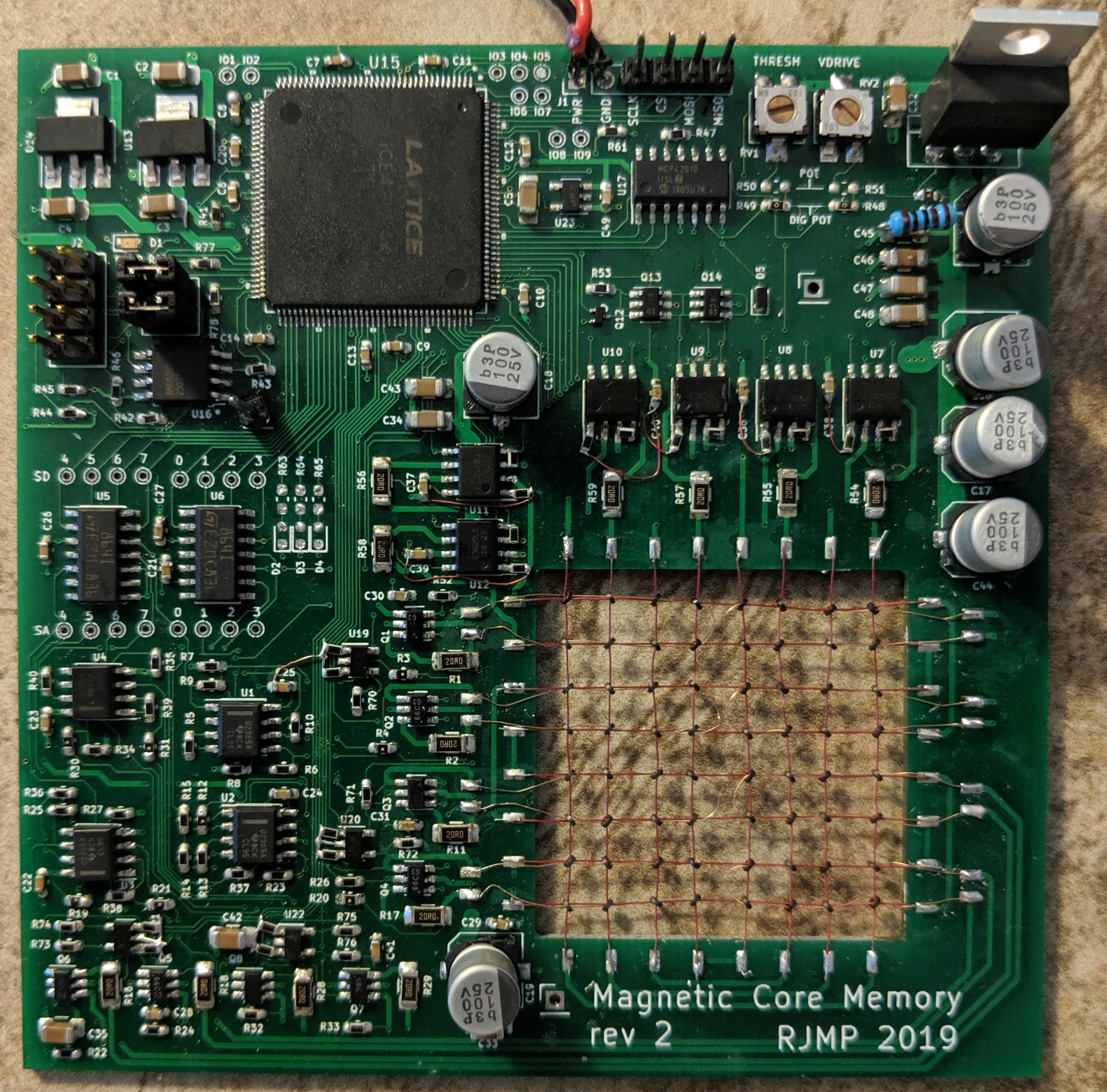
64 Bit Core Memory Array
I decided to build a modern version of an old-school core memory, for fun and to learn how they work. This article is about the design of the final memory array using a Lattice ICE40 FPGA as a SPI slave memory controller.
I previously wrote about the single bit prototype, and ferrite testing/seletion that led to this. I'm not inventing anything new here, and I'm not going to go too much into how a core memory works. There's lots of good resources out there for that. See the links in the "Resources" section if you want to get more background.
Array Structure
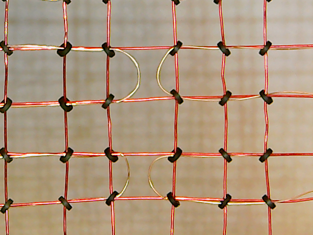
The array of ferrite cores is laid out in an 8x8 array, with 8 SENSE wires. This means that with each read/write, 8 bits are accessed at once, so not only is the physical layout an 8x8 grid, the memory is accessed as 8 addresses, each storing 8-bit words. There's nothing particularly special about this layout, it could be done other ways. You could do it with 1 sense wire for all of the bits, or 2, or 4, etc. You could even layout a 64-bit array with a single drive wire, and 64 SENSE wires. I don't claim this is optional; I could for example have added two extra row drivers, and removed 4 SENSE wires to make a 16x4-bit memory, and this would have required fewer parts overall.
I was concerned about how hard it would be to weave the array, but that actually turned out to be surprisingly easy. I just soldered one end of the column wires onto the pads, put a ferrite on each wire, then ran the first row wire through them. Then add the next row of ferrites, and run the next row wire, and so forth 8 times. It went quite quick.
Drive Circuits
I went through a couple iterations of the drive circuit. When I was first designing this, one of the main requirements was flexibility. I knew I would want to use a variety of different ferrite cores, and I didn't know how much current would be necessary or e.g. how much the required current might change with temperature. I actually envisioned needing an automated calibration process to adjust the drive current and sense threshold voltage, so I wanted the controller to have the ability to adjust both of those parameters.
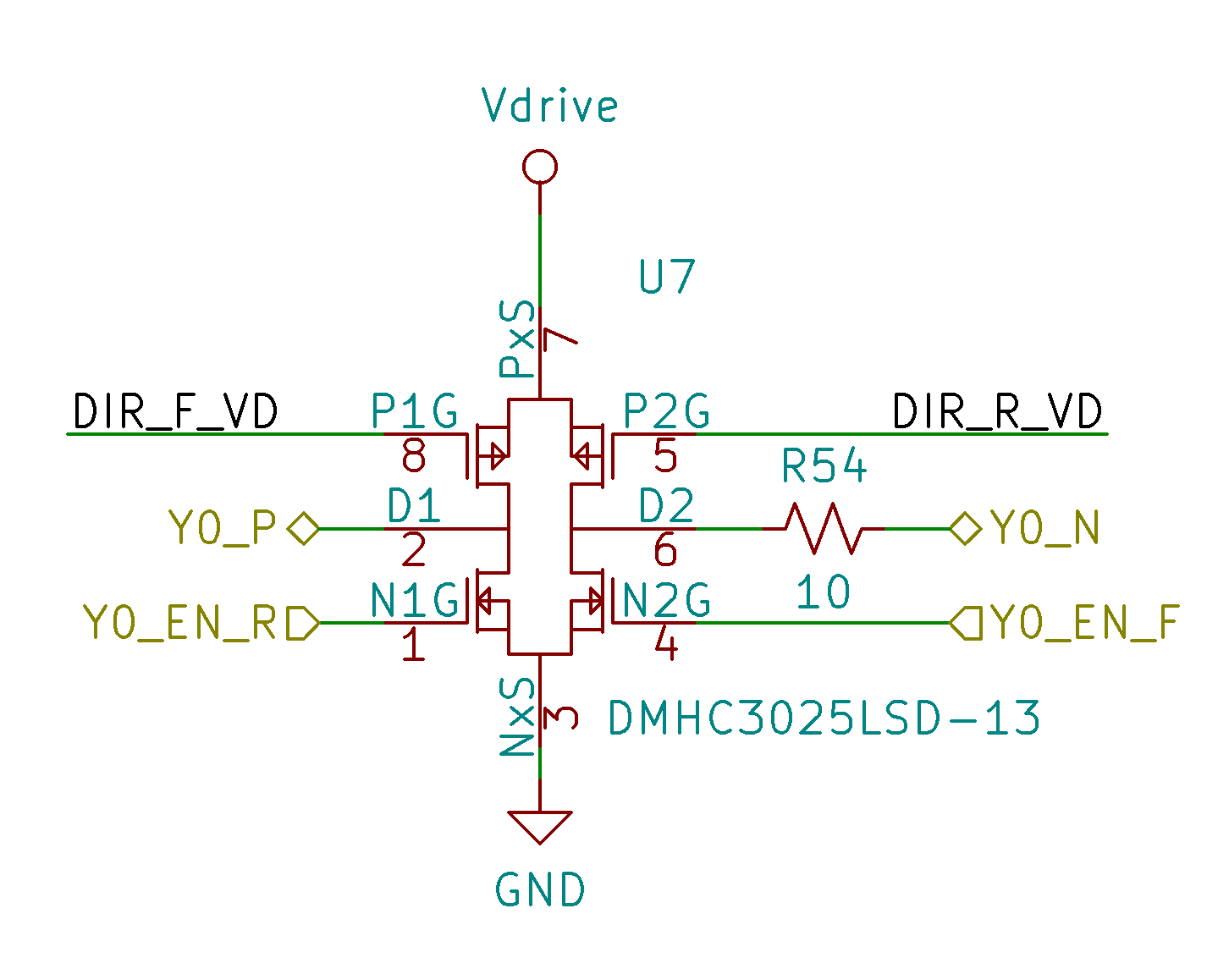
My first take at the drive circuit involved a sense resistor and an op-amp to do feedback control of the current. This had two main problems: 1) it required a lot of parts per drive wire, and 2) it made for slow and less predictable current edges1. It became clear that this was more complicated than it needed to be. Instead, I switched to the design below, which uses a single adjustable regulator to control the drive voltage, and a current limiting resistor. There's one of these for each row/column wire (6 total).
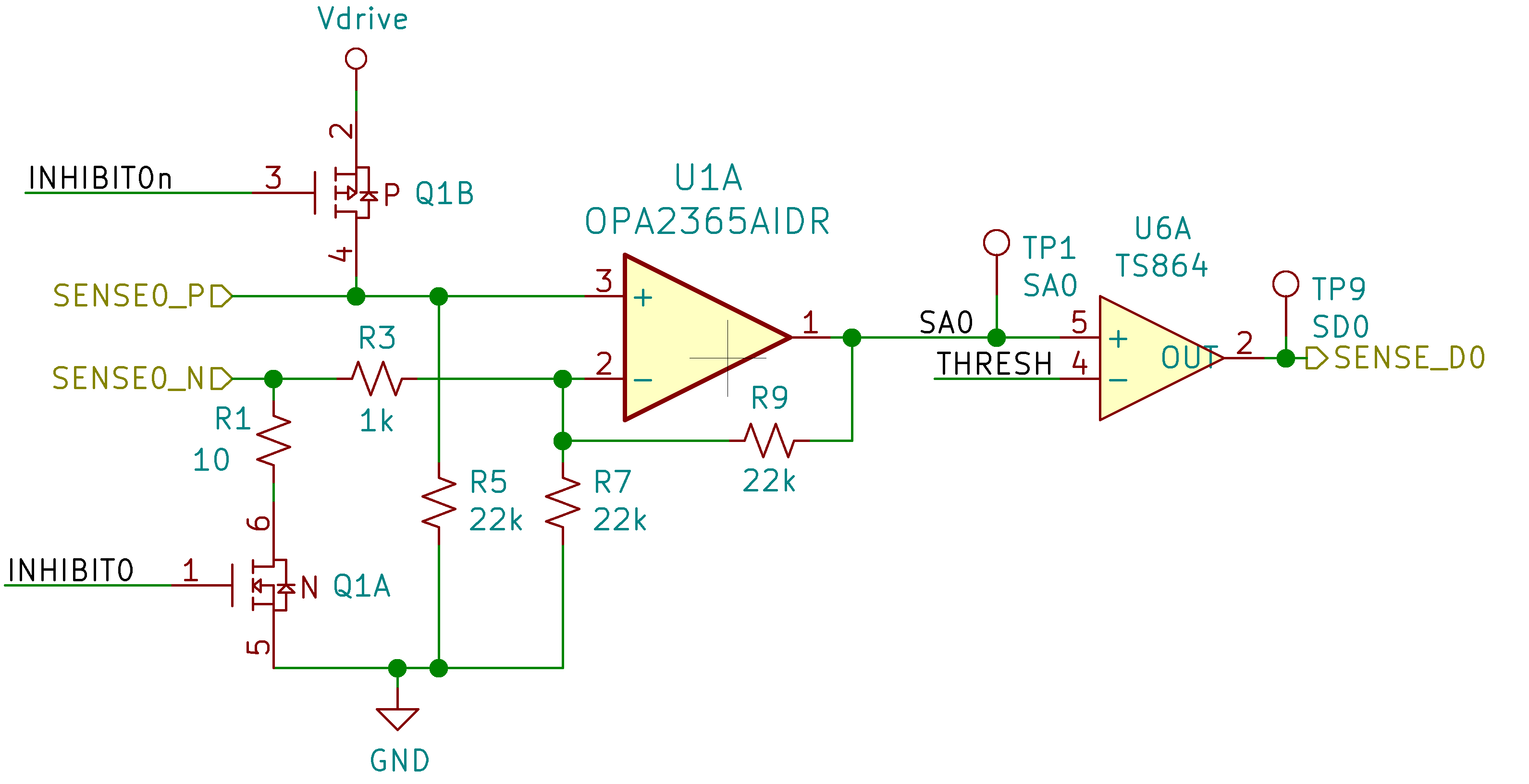
For each sense wire, the following circuit is replicated. The sense wires double as "inhibit" wires to control which bits are written during a write, so they also have FETs to enable this current. Unlike the row/column drivers, at least the inhibit current does not have to be bi-directional. The op-amp amplifies the small pulse voltage from the sense wire, and this is then fed to a comparator to threshold this signal and generate a 3.3V digital signal. The threshold voltage is controlled by a digital pot, so that it can be adjusted from software.
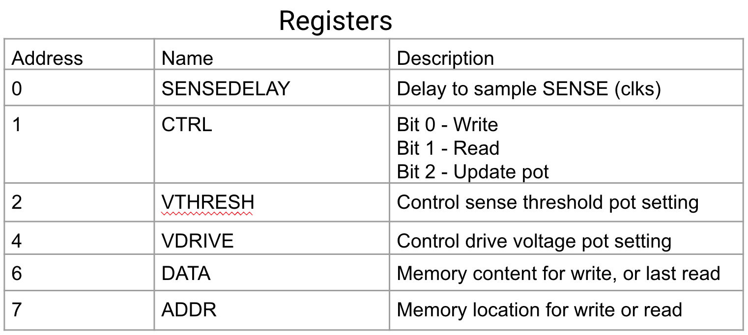
Controller
The controller is an ICE40 FPGA. I decided to set this up so that the core memory would be controlled by a SPI master (e.g. any microcontroller or an FTDI FT232H), so the job of the FPGA is to act as a SPI slave and drive the control signals to the memory circuits, as well as the digital potentiometer that controls the Vdrive regulator and the sense threshold voltage.
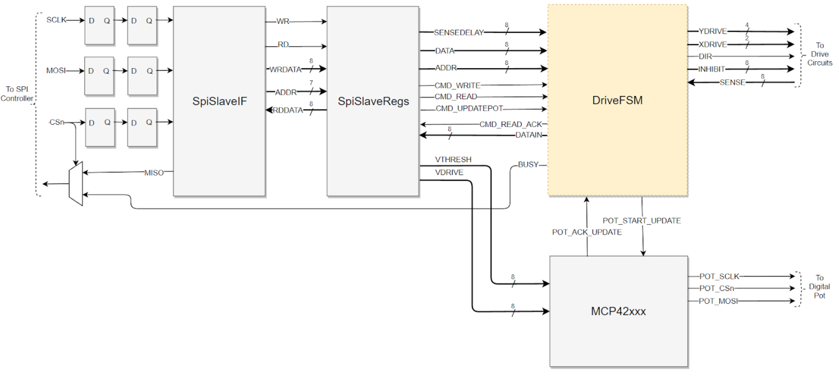
This project provided an opportunity for me to try out some new-to-me FPGA design tools. I used Chisel as a description language, cocotb for python testbenches, and the IceStorm open source project to generate bitstreams for the ICE40. I've always hated writing complex testbenches in verilog, and I found cocotb to be a pretty great alternative. I won't go into it too much, but the ability to add some flexibility, abstraction and re-usability to testbenches is pretty compelling. All I can say about IceStorm is that it worked fast and flawlessly for me, which is pretty amazing considering reverse engineering that had to go into making it work. Chisel is cool, and I can definitely see how it could be useful for larger projects, especially if they need configurable RTL generation. For this project, it definitely made things slower not faster. I don't love bringing a new programming language (Scala) and java runtime into my FPGA workflow, and for this project I think I ended up writing essentially the same thing in Chisel that I would have in verilog.
Source
PCB design (kicad): https://github.com/mcbridejc/core-mem-pcb
FPGA design: https://github.com/mcbridejc/core-mem-controller
Resources
https://en.wikipedia.org/wiki/Magnetic-core_memory
https://rolfebozier.com/archives/113
http://www.corememoryshield.com/
Conclusion
There's a great irony (absurdity?) in this project, in the fact that the FPGA I'm using to control a 64-bit memory array has about 80kbits of RAM built into it. Still though, a project like this is really more about the process than the final output. This was a great excuse to try a bunch of new things, practice some rusty analog design skills, and to understand ferromagnetic materials a bit better. I think I will be writing one more article in this series later, to discuss the Dash based python GUI for testing/controlling the core memory using an FTDI breakout as USB-to-SPI master. It's only tangentially related to core memory, but I've been thinking that a slightly modified version of Dash could be a really great way to build the "embedded device dashboard" GUI apps that I'm regularly wanting to build quickly.
Footnotes
- In the op-amp current controller, the op-amp output drive the base of an NPN transistor. Once the output got below about 0.7V (Vbe-on), the feedback loop for the op-amp is disconnected. I found that sometimes the op-amp output would stay around 0.7V, and sometimes it would drift down to 0V, and this meant that different channels could be starting from different voltages, and the slew rate of the op-amp is slow enough to matter here.↩